
1. What Is a Flying Probe Test?
A flying probe test is a computer-driven, non-destructive electrical testing method that utilizes multiple independently moving mechanical probes to contact test pads and traces on a printed circuit board.
Why Choose Flying Probe Testing?
Flying probe testing provides flexible electrical inspection without a dedicated bed-of-nails fixture. It is particularly useful for prototypes, small batches, and designs that change frequently.
- Lower initial tooling costs: Avoids the expense of a custom electrical test fixture.
- Flexible design updates: Test programs can be revised to accommodate board changes.
- Faster preparation: speed test can proceed without waiting for needle-bed fixture fabrication, once programming and validation are complete.
- Useful fault diagnosis: Helps locate opens, shorts, and supported component-related defects.
Its suitability depends on test access, required coverage, and production throughput.
Bare PCB Testing vs. PCBA Testing
Flying probe testing can be applied to bare printed circuit boards and assembled boards, but these are different tasks.
| Aspect | Bare PCB flying probe testing | PCBA flying probe testing |
|---|---|---|
| Test object | Conductive board structure before component assembly | Board with installed components |
| Main purpose | Check specified electrical connections and isolation | Check accessible connections and supported component characteristics |
| Program inputs | Board geometry, connectivity data, and test requirements | Connectivity and geometry, plus relevant component and assembly information |
| Main constraints | Accessible features and the required electrical test conditions | Probe access, circuit interactions, component properties, and system capabilities |
| Meaning of a pass | Executed bare-board checks meet their limits | Executed assembly checks meet their limits |
2. How Flying Probe Testing Works: Step-by-Step Mechanism
Understanding how flying probe tester works for pcb assembly requires looking at the synchronization between precision mechanical motion control and electrical measurement circuitry.
- Netlist and CAD Integration: The test system ingests board layout files, component placement data, and electrical netlists to map every connection point across the coordinate plane.
- Multi-Axis Probing: High-speed servo motors drive multiple independent probes (typically two to four or more) across the X, Y, and Z axes. These probes touch down simultaneously or sequentially on target test pads and component leads.
- Multi-Parameter Electrical Scanning: The tester applies low-voltage signals or small currents to verify continuity (detecting opens and shorts), measure passive component values (resistors, capacitors, and inductors), and check the polarity or forward-voltage drop of diodes and transistors.
- Automated Defect Isolation: By scanning the entire netlist, the system instantly flags broken traces, inadvertent solder bridges, missing components, or incorrect part values with high spatial accuracy.

3.What Can Flying Probe Testing Detect—and Miss?
Flying probe testing can identify electrical defects at accessible test points, but its coverage depends on the board, equipment, and validated test program.
| It can detect or evaluate | Conditions and limitations |
|---|---|
| Open circuits and shorts | Relevant connections must be accessible and included in the program. |
| Incorrect resistor, capacitor, or inductor values | Supported measurements must account for surrounding circuit paths. |
| Missing or incorrectly oriented components | Detection depends on electrical signatures or available optical functions. |
| Some connection and soldering defects | The defect must produce a detectable electrical response. |
| Selected powered-circuit behavior | Requires suitable equipment, connections, and dedicated tests. |
Flying probe testing may miss inaccessible connections, defects masked by parallel circuit paths, intermittent faults that do not occur during testing, and structural solder-joint problems that remain electrically conductive.
4.Flying Probe Test Point Design Guidelines
Flying probe test points should provide reliable electrical contact and enough clearance for safe probe movement. Confirm layout requirements with the test provider before releasing the PCB, because acceptable dimensions depend on the equipment and probe configuration.
- Provide accessible contact areas. Use suitable exposed pads, component pads, or untented vias approved by the test provider. Keep intended contact areas clear of solder mask and other insulating coatings.
- Confirm pad size and spacing. Select dimensions that accommodate the probe tip and positioning tolerances. Avoid applying one universal minimum to every tester.
- Allow clearance around components. Tall connectors, shields, and nearby components can obstruct the probe’s approach even when the pad appears accessible in a two-dimensional layout.
- Maintain alignment and board support. Provide visible fiducials and suitable clamping or support areas. Board movement and deflection can cause inconsistent contact.
- Plan access to important networks. Review test coverage during layout. Where direct contact is unavailable, agree on an alternative test method or document the coverage limitation.
- Provide complete design data. Supply consistent connectivity, placement, component-height, and board-revision information so the test provider can verify access and develop the program.
Test-point dimensions, surface-finish compatibility, and permitted contact locations should be approved for the actual board and testing process.
5.How to Read a Flying Probe Test Report
A flying probe test report shows whether the executed electrical checks met their programmed limits. Review the test scope and exclusions alongside the overall PASS or FAIL result.
| Report item | What to check |
|---|---|
| Board identification | Confirm the part number, design revision, serial number or batch matches the tested board. |
| Program version | Verify that the test program matches the released design and assembly variant. |
| Test results | Distinguish passed, failed, skipped, and untested items. Untested items are not confirmed passes. |
| Measurements and limits | Compare recorded values with the specified limits and units. |
| Failure location | Look for component references, network names, or coordinates that support troubleshooting. |
| Coverage | Check whether the percentage refers to networks, components, contact points, or defined faults, including its exclusions. |
| Retest history | Review the original failure, corrective action, and subsequent result. |
A failure may indicate a board defect, unreliable probe contact, or a program-related issue, so investigate before replacing components. Likewise, a PASS confirms only the checks performed; it does not automatically establish complete functionality or long-term reliability.
6.False Failures, Probe Contact, and Troubleshooting
Investigate Contact and Positioning First
Check whether the probe contacted the intended feature. Review alignment, board support, surface contamination, and probe condition.
Review the Program and Circuit Conditions
Confirm the board revision, assembly variant, component information, and test limits.
Also check whether the test conditions account for the surrounding circuit. A limit should be supported by engineering requirements and validated measurement behavior.
Maintain Probes According to the Equipment Requirements
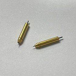
Needle wear, damage, or contamination can affect contact quality. Cleaning and replacement procedures should follow the equipment manufacturer’s instructions.
Confirm replacement-probe compatibility using the correct equipment model and part identification. Similar appearance does not establish equivalence.
Control Retesting
Retesting should follow a documented procedure. Repeating a measurement until it passes can hide an unresolved problem.
Record what changed between attempts, such as cleaning, repositioning, probe replacement, program correction, or board repair.
7.Flying Probe vs. ICT: Compare Cost and Production Fit
In this comparison, ICT refers to a conventional bed-of-nails in-circuit test arrangement. Flying probe platforms can themselves perform forms of in-circuit testing, so the distinction concerns the contact method as well as the selected system capabilities.
| Decision factor | Flying probe testing | Bed-of-nails ICT |
|---|---|---|
| Electrical contact arrangement | Movable probes | Dedicated fixed probe fixture |
| Initial investment per design | Programming, validation, and any required support | Programming, validation, and fixture development |
| Design changes | Often addressed through program changes, subject to access | May require fixture modification as well as program changes |
| Production cycle | Depends on movement, measurements, and handling | Can provide short cycles for suitable applications |
| Maintenance | Moving system, probes, and contact verification | Fixture pins, interfaces, and contact verification |
| Selection basis | Product mix, coverage, throughput, and change frequency | The same factors, including fixture economics |
8.Flying Probe Testing FAQ
Can flying probe testing inspect BGA connections?
It may evaluate accessible networks connected to BGA terminals, and some systems support additional techniques. Detection depends on the circuit, access, and equipment. Do not assume complete coverage of hidden joints.
Can testing proceed without the original CAD files?
Some providers offer alternative-data or reverse-engineering workflows. Their feasibility, preparation effort, and validation requirements need to be confirmed for the specific board.
Do flying probes leave marks on the PCB?
Contact can leave marks depending on the probe, surface, and contact conditions. Their acceptability should be assessed against the product requirements rather than assumed from the presence or absence of a visible mark.
Is flying probe testing suitable for high-volume production?
It can be, depending on the equipment, test sequence, handling system, and required output. Evaluate measured throughput for the intended product rather than relying on a general small-batch label.
What should I provide for a flying probe test quotation?
Provide the board type, released design data, relevant assembly information, quantities, testing objectives, reporting requirements, and delivery schedule. Ask the provider to identify required files, expected coverage, exclusions, and program-development charges before placing the order.
 Russian
 English
 German
 French
 Spanish
 Vietnamese