
Copper thickness measurement determines the thickness of a copper layer at a defined location using a method suited to the material, geometry, and manufacturing stage. In PCB production, the measurement may concern incoming copper foil, surface traces, or copper deposited inside plated through-holes.
1. PCB Copper Thickness and Conversion Charts
PCB copper thickness is commonly specified in ounces per square foot (oz/ft²), micrometers (μm), millimeters (mm), or mils. Copper weight describes mass per unit area, while the other units describe physical thickness.
For quick reference, 1 oz copper is approximately 0.035 mm thick, and 2 oz copper is approximately 0.070 mm thick.
PCB Copper Weight-to-Thickness Chart
| Copper weight | Thickness (μm) | Thickness (mm) | Thickness (mils) |
|---|---|---|---|
| 0.5 oz/ft² | 17.4 | 0.0174 | 0.685 |
| 1 oz/ft² | 34.8 | 0.0348 | 1.370 |
| 2 oz/ft² | 69.6 | 0.0696 | 2.740 |
| 3 oz/ft² | 104.4 | 0.1044 | 4.110 |
| 4 oz/ft² | 139.2 | 0.1392 | 5.480 |
| 6 oz/ft² | 208.8 | 0.2088 | 8.220 |
Copper Thickness Unit Conversion Chart
| Conversion | Formula |
|---|---|
| Micrometers to millimeters | mm = μm ÷ 1,000 |
| Millimeters to micrometers | μm = mm × 1,000 |
| Mils to micrometers | μm = mils × 25.4 |
| Micrometers to mils | mils = μm ÷ 25.4 |
| Copper weight to nominal thickness | μm ≈ oz/ft² × 34.8 |
| Nominal thickness to copper weight | oz/ft² ≈ μm ÷ 34.8 |
For example, a nominal copper thickness of 70 μm equals 0.070 mm, or approximately 2.76 mils. It is commonly associated with a 2 oz copper specification; the small difference reflects rounding.
Base Copper vs. Finished Copper Thickness
Base copper is the starting foil thickness. Finished copper is the thickness remaining after the applicable manufacturing processes.
Plating adds copper, while cleaning and microetching can remove it. Consequently, the final thickness depends on the process route and measurement location. Inner-layer copper and plated outer-layer copper should not be evaluated using the same assumptions.
Copper Thickness vs. Overall PCB Thickness
Copper thickness describes an individual conductive layer. Overall PCB thickness includes the board’s dielectric materials and copper layers, with the measurement definition specified by the supplier or drawing.
2.How to Measure Copper Thickness on PCB
To measure copper thickness on a PCB, first identify whether you are checking surface copper, plated-through-hole copper, or an internal layer. Then select a method suitable for that feature and compare the results with the specified requirements.
1. Identify the Copper Feature
Confirm the measurement location and manufacturing stage. Base copper, finished surface copper, and hole-wall plating are different measurement targets.
Also check whether the copper is exposed or covered by solder mask, OSP, ENIG, or another finish. A method suitable for bare copper may not work correctly through additional layers.
2. Select the Measurement Method
| Measurement target | Method to evaluate | Main consideration |
|---|---|---|
| Exposed surface copper or traces | Microresistance gauge | Supported trace dimensions, contact area, and surface condition |
| Plated-through-hole copper | Dedicated hole-copper gauge, such as an appropriate eddy-current configuration | Hole diameter, board thickness, and probe compatibility |
| Internal copper or local hole-wall structure | Microsection analysis | Destructive preparation and representative section location |
| Separate copper foil | Suitable foil gauge or precision mechanical measurement | Resolution, contact pressure, and foil condition |
3. Prepare and Verify the Equipment
Inspect the probe and sample, select the correct instrument settings, and perform the reference check required by the manufacturer.
Use approved preparation methods. Scraping or polishing a measurement area can remove copper and change the result.
4. Measure at Defined Locations
Position the probe according to the instrument instructions and obtain a stable reading. Repeat measurements with repositioning where required by the inspection procedure.
Measure the locations specified in the sampling plan. A single reading cannot establish thickness uniformity across the board.
5. Record and Evaluate the Results
Record individual readings, units, locations, board identification, and instrument configuration. Compare results with the approved drawing or acceptance specification.
3. IPC Copper Thickness Standards and Acceptance Criteria
Manufacturing tolerances can significantly alter the final cross-sectional profile of a circuit board. When determining what thickness is acceptable for production release, fabricators and quality engineers must adhere strictly to established industry specifications.
- IPC-6012 and IPC-2152 Compliance: These standards dictate the minimum acceptable copper plating thickness inside plated through-holes (PTH) and on external/internal conductive planes. Complying with these benchmarks ensures structural integrity under thermal shock.
- Accounting for Etching Undercut: During chemical etching, the sideways erosion of copper reduces trace cross-sections. Standard manufacturing margins account for this variance to ensure that a nominal pcb thickness or trace profile maintains its rated electrical performance.
- Typical Design Targets: A typical pcb thickness for standard double-sided or multi-layer boards is 1.6mm, with outer copper layers specified at 1 oz or 2 oz depending on thermal management requirements.
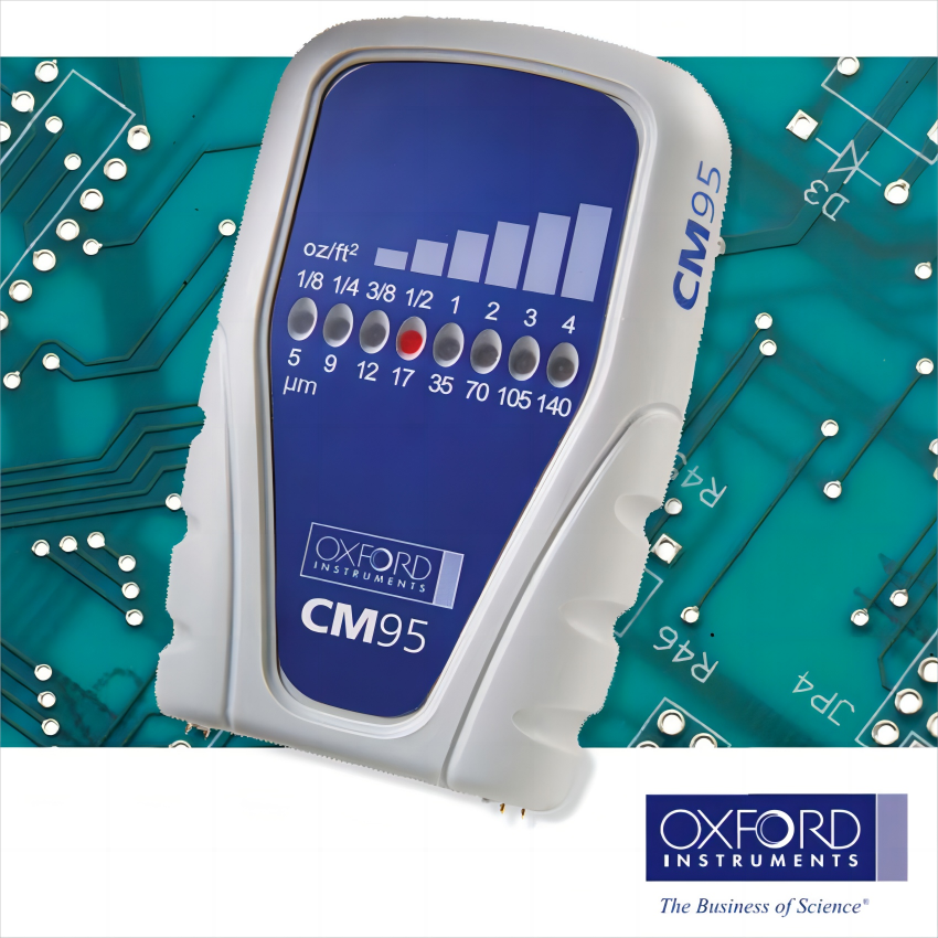
4.Copper Thickness Measurement Methods Compared
The correct method depends on access to the copper, sample geometry, and the information required.
Microresistance Measurement
Microresistance instruments use an electrical resistance measurement to determine copper thickness within their supported application conditions.
They are used for applications such as copper foil, exposed surface copper, and suitable traces. Probe arrangement, conductive geometry, and contact conditions matter.
Hitachi identifies microresistance as the technology used by several of its PCB surface-copper instruments. Its application chart also distinguishes surface measurement from through-hole measurement.
Eddy-Current Measurement
Dedicated eddy-current configurations are available for plated-through-hole copper measurement.
The instrument and probe must suit the hole geometry and application. Support for one through-hole size does not establish suitability for blind vias, microvias, or every board thickness.
Hitachi’s CMI511 documentation identifies eddy-current technology for through-hole copper, while its CMI760 platform combines technologies for different copper measurement tasks.
Microsection Analysis
Microsection analysis involves preparing a cross-section and examining the exposed structure with suitable microscopy.
It can provide local evidence of copper thickness and the surrounding structure. However, sample preparation and section location affect what is observed. A single section does not demonstrate uniformity across an entire panel.
Microsectioning is destructive to the sectioned specimen, so production inspection may use designated coupons or selected samples where appropriate.
Other Conditional Methods
X-ray fluorescence, surface profilometry, and mechanical measurement can be useful in suitable applications, but each has limitations.
XRF requires a supported layer model, thickness range, and measurement configuration. Profilometry requires a meaningful reference surface or step. A micrometer may be appropriate for accessible, independent foil or sheet if its resolution and contact conditions suit the material.
| Method | Potential application | Sample impact | Main limitation to verify |
|---|---|---|---|
| Microresistance | Exposed surface copper, foil, suitable traces | Normally non-destructive within approved use | Contact and conductive geometry |
| Eddy current | Supported plated-through-hole applications | Normally non-destructive | Hole geometry and probe configuration |
| Microsection | Local surface, internal-layer, or hole-wall evaluation | Destructive to the specimen | Preparation quality and section location |
| XRF | Supported copper coating or multilayer applications | Normally non-destructive | Layer model, substrate, and thickness range |
| Profilometry | Accessible copper step or feature | Depends on preparation | Reference surface and feature geometry |
| Mechanical measurement | Independent copper foil or sheet | Usually non-destructive, subject to handling | Resolution, compression, and accessibility |
5.How to Choose a PCB Copper Thickness Gauge
Selecting the right PCB copper thickness gauge requires evaluating four core dimensions based on your specific testing requirements, measurement technology, equipment form factor, and performance metrics:
- Identify Measurement Objectives (What to Measure):
- Clearly distinguish whether you are measuring surface foil and outer traces, plated through-hole (PTH) barrel copper, encapsulated inner layers, or final surface platings. Each area demands specialized probes and instrumentation.
- Select the Appropriate Measurement Technology:
- Surface Eddy Current / Microresistance Gauges: Ideal for rapid, non-destructive surface copper screening on production lines and incoming quality control (IQC) docks.
- Specialized PTH Eddy Current Hole Gauges: Utilize fine needle probes inserted directly into drilled holes to precisely quantify vertical barrel plating thickness.
- X-Ray Fluorescence (XRF) Analyzers: Best for high-precision, non-destructive micro-analysis of multi-layer surface finishes and thin metal platings (such as ENIG or immersion silver).
- Evaluate Equipment Form Factors & Environment:
- Handheld / Portable Units: Highly flexible for shop floor use, plating line monitoring, and receiving inspection.
- Benchtop Systems: Designed for metrology laboratories and QA centers requiring advanced accuracy and automated multi-point mapping.
- Assess Key Performance Criteria:
- Verify that the measurement range covers your specific product specs, look for automatic temperature compensation (vital for inspecting hot panels straight out of plating baths), check for data logging and SPC export capabilities, and ensure ease of calibration against reference standards.
6.Calibration and Common Measurement Errors
Calibration establishes the relationship between an instrument’s indications and reference values under stated conditions. A routine verification checks whether the system continues to meet the specified criteria. Adjustment changes the instrument response.
When readings become inconsistent, investigate systematically:
- Sample condition: Check contamination, oxidation, coatings, or damage.
- Contact and positioning: Confirm stable contact and the correct measurement location.
- Geometry: Verify that traces, edges, holes, and board dimensions meet the application requirements.
- Temperature: Check sample conditions and the instrument’s compensation limits.
- Probe condition: Inspect for wear, damage, or connection problems.
- Settings and references: Confirm the application setup and reference-standard status.
Repeated readings can be tightly grouped and still be biased. Repeatability alone does not demonstrate accuracy.
7.Copper Thickness Measurement FAQ
What thickness is 1 oz copper in millimeters?
One ounce of copper per square foot corresponds to approximately 0.035 mm of uniform copper. This is a nominal conversion, not a universal finished-board acceptance limit.
What is the difference between base copper and finished copper thickness?
Base copper refers to the raw weight of the copper foil supplied on the unetched laminate (e.g., 1 oz). Finished copper thickness includes the base foil plus additional copper deposited during subsequent pattern plating and through-hole barrel plating processes, making the final measured thickness significantly greater than the raw foil specification.
Does making copper thick improve every PCB?
No. Increasing copper thickness can support electrical and thermal objectives, but it also affects fabrication and layout requirements. Select thickness together with trace geometry, operating conditions, and manufacturing capability.
Can copper thickness be measured without cutting the board?
Yes, where a suitable non-destructive instrument supports the sample and application. Such measurements do not replace every structural assessment that a cross-section can provide.
Can one probe measure surface copper, hole copper, and internal layers?
Do not assume so. These are different measurement tasks. Some instruments support multiple applications through separate configurations, while inaccessible internal layers may require microsection analysis or another specifically validated method.
 Russian
 English
 German
 French
 Spanish
 Vietnamese