
1. What Is ENIG Surface Finish?
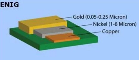
ENIG Surface Finish (Electroless Nickel Immersion Gold) is a two-layer metallic surface finish used on printed circuit boards (PCBs). It protects copper traces and provides a reliable surface for soldering and wire bonding
Key Characteristics:
- Three-Layer Structure:
- Base Copper (Cu): The underlying circuit trace foundation.
- Electroless Nickel Layer (3.0-6.0μm): Acts as a diffusion barrier preventing copper migration and serves as the mechanical base for solder joints.
- Immersion Gold Layer (0.05-0.10μm): A micro-thin protective coating that prevents the nickel from oxidizing during storage and dissolves instantly during SMT reflow.
- Core Benefits:
- Exceptional Flatness: 100% coplanar surface, making it ideal for fine-pitch components like BGAs, QFNs, and micro-passives.
- Long Shelf Life: Maintains solderability for 12 months or more when stored properly in vacuum packaging.
- Wire Bonding & Contact Support: Pure gold surface supports gold wire bonding and light mechanical contact applications.
2. ENIG Manufacturing Process and Thickness Standards
The ENIG plating process requires strict chemical control across multi-stage wet-bench lines to ensure uniform deposition and compliance with industrial benchmarks like IPC 4552 ENIG specifications.
- Surface Pre-Cleaning & Micro-Etching: Alkaline cleaners remove organic contaminants, followed by micro-etching to establish ideal copper surface topography for nickel adhesion.
- Catalytic Activation: Palladium or similar catalysts are seeded onto the copper surface to initiate the autocatalytic nickel deposition reaction.
- Electroless Nickel Deposition: The board is immersed in a hypophosphite-reduced nickel bath. The chemical reduction creates a uniform nickel-phosphorus alloy layer. Precise control over bath temperature and pH regulates the phosphorus content (typically maintained between 7% and 10% [Data needed: exact proprietary bath parameters per manufacturer]) to prevent structural defects.
- Immersion Gold Deposition: The nickel-coated board enters an immersion gold bath. Gold ions spontaneously displace surface nickel atoms until a continuous, protective gold layer of standard ENIG gold thickness (0.05–0.1μm) is achieved.
- Post-Rinse & Drying: Thorough deionized water rinses remove residual ionic contaminants before low-temperature drying.
3.ENIG Black Pad and Other Finish Problems
ENIG black pad is associated with excessive nickel corrosion during gold deposition and can compromise solder-joint integrity.
A sound investigation separates the observed symptom from the proposed cause.
| Observed problem | Possible causes to investigate | Evidence to collect | Appropriate next step |
|---|---|---|---|
| Poor solder wetting | Contamination, pad condition, flux compatibility, thermal process | Lot records, solderability results, paste details, profiles | Compare affected and unaffected samples |
| Brittle joint separation | Nickel corrosion, interface defects, mechanical loading | Fracture surfaces and appropriate laboratory analysis | Confirm the failure mechanism |
| Uneven finish appearance | Local contamination, process variation, handling | Surface inspection, thickness map, production records | Evaluate against acceptance criteria |
| Intermittent test contact | Probe condition, alignment, force, surface contamination | Controlled repeat measurements and fixture checks | Separate contact errors from circuit defects |
| Problems after later assembly | Thermal history, delays, remaining pad condition | Complete production timeline and final-stage results | Reassess the affected process sequence |
Prevention Requires More Than a Thickness Check
Thickness measurements provide useful evidence, but corrosion evaluation addresses a different question.
Chemical supplier welleltron describes inspection and rating methods intended to distinguish limited corrosion from conditions that threaten finish performance. Apply the criteria of the governing standard and revision rather than mixing acceptance rules from different documents.
4. ENIG Shelf Life, Storage, and High-Frequency Signal Integrity
Maximizing the operational window of an enig pcb requires proper shop-floor management:
- Storage Environment: Store boards in vacuum-sealed moisture barrier bags with desiccants at controlled room temperatures (RH < 60%).
- High-Frequency & RF Considerations: The nickel layer in ENIG possesses ferromagnetic properties. In high-frequency microwave and RF circuit designs, the skin effect concentrates high-frequency currents within the nickel layer, leading to higher insertion loss and signal attenuation compared to bare copper or silver finishes. RF designers must factor this magnetic attenuation into high-speed transmission line simulations.
5. Frequently Asked Questions About ENIG Surface Finish
Q1: What is the exact thickness standard for ENIG per IPC-4552?
A: According to IPC-4552 specifications, the standard nickel thickness ranges from 3.0 to 6.0μm (118-236μm), while the immersion gold layer should measure between 0.05 and 0.10μm (2-4μm) to ensure optimal wetting without triggering black pad corrosion.
Q2: Can ENIG boards be pre-baked before SMT assembly like HASL boards?
A: Yes, ENIG boards generally tolerate standard moisture-removal bake cycles (120℃) better than OSP boards because the metallic gold and nickel layers do not oxidize or degrade under moderate thermal exposure.
Q3: How can quality engineers detect a black pad defect before soldering?
A: Non-destructive optical inspection cannot detect black pad. Quality labs rely on destructive cross-sectioning combined with Scanning Electron Microscopy (SEM) and Energy Dispersive X-ray Spectroscopy (EDS) to analyze nickel-phosphorus grain boundary integrity.
Q4: Can ENIG Be Used for Wire Bonding?
A: yes. IPC-4552B identifies aluminum and copper wedge wire bonding among ENIG applications. This does not establish universal compatibility with every wire material or bonding technique.
 Russian
 English
 German
 French
 Spanish
 Vietnamese