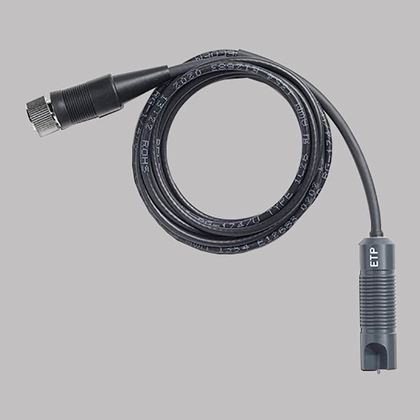
Hitachi CMI700 ETP probe
$700.00
Hitachi CMI700 ETP probe is a high-precision, non-destructive electrical thickness probe that uses micro-resistance technology to accurately measure copper and conductive coating thickness on printed circuit boards, including surface and through-hole plating.
Hitachi CMI700 ETP probe Overview
Hitachi CMI700 ETP probe(Electromagnetic Through-hole Probe) is a specialized sensor designed specifically for the Surface Finishing Industry and Printed Circuit Board (PCB) inspection. Unlike standard surface probes that measure flat areas, the PTH hole ETP probe is engineered to enter small-diameter holes and measure the thickness of the copper barrel.
Compatible with the Oxford CMI500 and the newer Hitachi CMI700 series, this ETP probe for CMI500 systems addresses the industry’s need for Non-Destructive Testing (NDT). It allows manufacturers to verify plating quality without sectioning the board, thereby reducing waste and speeding up the Quality Control (QC) process.
2. Core Functionality: How the ETP Probe Works
The ETP probe operates on the principle of eddy-current induction. When the probe tip is inserted into a hole, it generates an electromagnetic field that induces eddy currents in the copper plating. The probe then measures the impedance change caused by these currents, which is directly proportional to the thickness of the copper.
Key Technical Advantages:
Surface Independent: The hole copper thickness probe is uniquely designed to ignore surface copper, focusing exclusively on the barrel of the hole. This is vital for boards where Circuit Board Plating may vary between the surface and the hole.
Measurement Range: Typically measures copper from 0.08 to 4.0 mils (2 to 100 μm).
Hole Size Compatibility: Available in various sizes, such as the ETP-1, to accommodate hole diameters as small as 31 mils (0.8 mm).
Substrate Versatility: Works effectively on double-sided and Multi-Layer Coating boards, ensuring High Precision Thickness readings across different laminate types.
3. Industrial Applications and Use Cases
The PCB hole copper ETP probe is an indispensable tool in several stages of the Electronics Manufacturing lifecycle:
Quality Control (QC) in PCB Fabrication
During the plating process, the Plating Thickness Testing must be verified to ensure the barrel wall meets the minimum design requirements. Failure to do so can lead to open circuits during the thermal stress of soldering.
Incoming Inspection
OEMs purchasing boards often utilize a Used CMI500 Gauge equipped with a Replacement ETP probe to audit the quality of their vendors’ shipments. This ensures that the PCB Coating Thickness adheres to IPC standards.
Surface Finishing Industry
For specialized boards requiring Solder Thickness Measurement or noble metal finishes, the ETP probe ensures the underlying copper foundation is solid before subsequent layers are applied.
4. Technical Characteristics and Data Precision
Reliable Probe Calibration is the foundation of accurate data. The ETP probe for Hitachi/Oxford systems relies on CMI500 Calibration Standards, which typically consist of NIST-traceable copper foil cylinders of known thickness.
Precision: The system offers a repeatability of ±0.01 mils (0.25 μm) for standard copper thicknesses.
Accuracy: Within ±5% of the calibrated standard.
Speed: Readings are instantaneous, allowing for 100% inspection of critical holes if required by ETP requirements.
Data Storage: When paired with the Oxford CMI500 or CMI700, data can be stored, averaged, and exported for statistical process control (SPC) reporting.
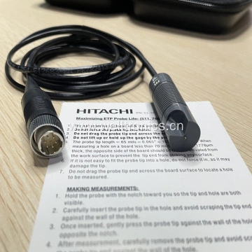
5. Maintenance, Repair, and Troubleshooting
Because the ETP probe is a mechanical device that physically enters holes, it is subject to wear and tear. Proper Hitachi probe maintenance is essential for longevity.
Troubleshooting ETP Probe Issues
If readings become erratic or the gauge displays errors, users should consult the CMI500 ETP operation manual. Common issues include:
Tip Contamination: Solder mask or debris inside the hole can interfere with the signal.
Damaged Ferrite: The delicate tip can crack if dropped. In such cases, CMI500 Probe repair or a Replacement ETP probe is necessary.
Calibration Drift: If the probe is dropped or exposed to extreme temperatures, it may require a fresh setup using the CMI500 Calibration Standards.


