1.What Is a PCB Test Point?
PCB test points are small, exposed metal pads or loops on a circuit board, designed for probes to easily access specific circuit points for signal injection, voltage/signal measurement, debugging, or automated testing (like In-Circuit Testing/Flying Probe) during manufacturing or repair, ensuring functionality without damaging the board 。
In simple terms, test points in PCB designs act as access nodes for measurement tools such as multimeters, oscilloscopes, flying probes, or in-circuit testers.
Common uses include:
- Voltage measurement
- Signal integrity checks
- Continuity testing
- Programming and calibration
- Fault isolation during Quality Control (QC)
2. Purpose and Function
The strategic inclusion of test points on pcb directly supports Testability (Design for Testability or DFT), making the board easier, faster, and cheaper to verify and repair.
- Quality Control (QC): During manufacturing, test points in pcb enable automated systems to quickly verify component placement, solder joint quality, and circuit continuity.
- Troubleshooting and Debugging: They provide critical access points for manual or automated diagnostics when a fault is detected. Engineers use them to check voltages, timing, and current flow.
- Performance Verification: Test points allow engineers to connect measurement instruments, such as oscilloscopes, to check signal characteristics (pcb oscilloscope test point), which is vital for pcb high speed test point applications.
3. Types of PCB Test Points
The form of a test point pcb depends on the testing methodology and the available board space:
| Test Point Type | Description | Common Application | Keywords |
| Pads/Vias | Simple circular or square Exposed Copper areas, sometimes utilizing existing test point pcb through hole vias. | Low cost pcb test points for flying probe testing. | test point on pcb, small pcb test points |
| SMD Terminals | Surface-mount components designed purely for probing. They often have a slightly raised profile. | Automated testing where a reliable surface contact is needed. | smd test points, pcb test point terminals, test point pcb footprint |
| Pins/Connectors | Robust physical components that are soldered in place. | High-reliability manual testing or connecting permanent cables (pcb test point connector). | pcb test point pins, test pin |
| Specialized Types | Features like the pcb test point loop or areas designed to mount pcb test point jumpers (short-circuit links). | Temporary modification of a circuit or easy current measurement. | pcb test point loop, mount pcb test point jumpers |
4. Application in Automated Testing: ICT Test Points
In high-volume manufacturing, automated testing is performed using the In-Circuit Test (ICT) method. This requires dedicated ict test points that are precisely positioned to align with the fixed probes of a “bed-of-nails” fixture.
- Design for ICT: These test points pcb must adhere to strict pcb test point guidelines regarding clearance and size to ensure all probes can make simultaneous and accurate contact.
5. PCB Test Point Design Guide
Implementing effective pcb test points requires adherence to best practices to maximize their usability:
- Accessibility and Clearance: Test points must be easily accessible by a test probe. Designers must consider test point spacing and avoid placing them under or too close to tall components.
- Size Specification: The pcb test point size must match the intended probe diameter. For instance, small pcb test points might be used for fine pitch flying probes, while larger pads are needed for ICT probes.
- Net Selection: Place test points on critical nodes (power rails, clock signals, chip I/O) to maximize diagnostic coverage.
- Signal Integrity: For high-speed lines, the pcb test point should be added with minimal impact on signal characteristics. A direct contact or a small loop is preferable to a long trace stub.
- Documentation: Clearly document the location and signal name of every test point pcb in the design documentation and silkscreen for rapid identification.
6.PCB Test Points Advantages
The upfront effort of adding test points pays dividends throughout the product lifecycle:
- Reduced Testing Time: Automated systems (ICT test points) can test a complex board in seconds.
- Lower Rework Costs: Early defect identification prevents complex, component-level repairs later.
- Field Serviceability: Makes the board easier to diagnose and repair in the field, extending product life.
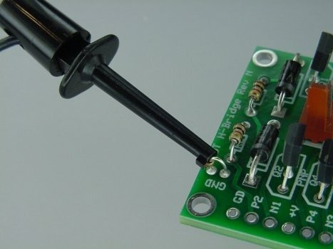
7. How to Use Test Points on PCB
Using test points is straightforward, depending on the phase:
- Automated Testing (ICT/Flying Probe): The PCB is loaded into a fixture that automatically contacts all test points simultaneously, measuring resistance, capacitance, and voltage according to a predefined program.
- Manual Debugging (Engineers): An engineer connects the ground lead of an instrument (like a multimeter or oscilloscope) to a known ground test point and then touches the signal probe to the target test point to read the voltage or waveform.
PCB test points are essential elements that bridge design, manufacturing, and quality assurance. From smd test points to pcb test point pins, thoughtful planning ensures effective testing without increasing cost or board complexity.