Knowledge Base

Explore the Knowledge Base

Certifications

Welleltron is NIST, IPC, & ISO certified, DLA approved, and ITAR registered. We have the UL seal of approval and have exceptional materials compliance and reporting.

Learn PCB

Knowing more about manufacturing processes will help you design cost-effective and robust boards. Check out our Learn PCB mini-blog to get guidelines and a look behind the fab curtains.

Defense & capabilities


Technical specs for aerospace and defense customers. Welleltron manufactures, assembles, and rigorously tests rugged, reliable IPC 6012 class 3/A PCBs in as fast as 2 days.

PCB design guides

The PCB design guides provide critical information to prevent delays and avoid unnecessary costs. From flex and HDI, to controlled impedance and DFM, we cover a vast range of topics.

Popular Learn PCB topics

Drawing a schematic of a circuit is the initial stage in PCB design. CAD software is then used to convert this block diagram into schematic drawings. A schematic is made up of component symbols and the connections that connect them. These nets will become copper traces on the circuit board.

PCB manufacturing involves converting design files which include Gerbers and netlists into a physical circuit board on which components can be placed and soldered.

PCB assembly transforms a fabricated circuit board into an electronic assembly by adding components such as resistors, capacitors, integrated circuits, and connectors.

PCB surface finish is a protective coating applied to exposed copper pads and other designated copper features on a printed circuit board. It helps preserve solderability before assembly and provides a suitable surface for the intended connection method.

While electronic components process information in form of electrical signals, a printed circuit board is the skeletal structure on which the electronic components are mounted and soldered to hold them together and provide pathways for information to flow between components through PCB traces.

Click here to change this text. Lorem ipsum dolor sit amet, consectetur adipiscing elit. Ut elit tellus, luctus nec ullamcorper mattis, pulvinar dapibus leo.

Our best blogs

Locating Pins

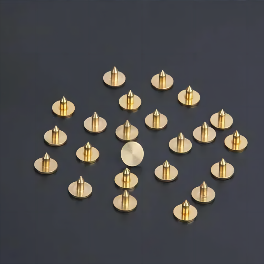
How to Choose PCB Locating Pins

Selecting Locating Pins material, tip geometry, or mounting tolerance results in mechanical binding, hole edge gouging, probe mis-hits, and premature pallet degradation.
Read More

Other ways Welleltron can help

PCB consumables
& Processes

Knowing PCB manufacturing processes and Consumables usage will help you produce circuit boards cost-effectively and efficiently.

Support

Need help with your stack-up? Want to find out what our products ? Have questions about your order? We’re here to help.

Talk to a Welleltron PCB Expert today

24 hours a day, 7 days a week.
Call us: +86 18680058386
Email us: carol@welltronics.cn