
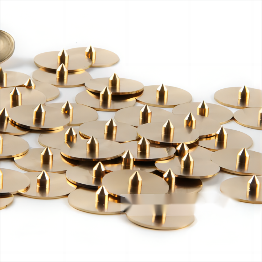
Locating pins, also commonly called alignment pins or tooling pins orregistration pins, are precision machined mechanical pins used to register and fix a PCB or PCBA onto a fixture, carrier, routing jig or test plate. They engage with non-plated tooling holes on the board to restrict movement and control positional repeatability during manufacturing, inspection or electrical testing.
1. PCB Locating Pins: Functions & Process Applications
Mechanical locating pins establish a repeatable Cartesian coordinate system (X, Y, Z) by engaging precision-drilled tooling holes (typically 3.0mm to 4.0mm) on the panel margin. Different PCB manufacturing stages place distinct physical demands on these components:
[ PCB Tooling Hole ] ---> Engages Locating Pin ---> Establishes Fixture Datum (X, Y, θ)
A. SMT Reflow Carriers & Solder Pallets
Pins must endure thermal cycling up to 260℃, resist chemical attack from aggressive fluxes, and accommodate differential thermal expansion between the FR-4 laminate and synthetic carrier materials (e.g., Durostone or Garolite) without causing panel bowing.
B. ICT and FCT Test Fixtures
Locating pins bear heavy downward spring loads exerted by hundreds of pogo pins simultaneously. They must prevent lateral micro-shifting ( ≤0.02mm) to keep test probes centered on tiny SMD test pads while providing electrical isolation where necessary.
C. CNC Routing and Depanelizing Jigs
During mechanical depanelization, pins absorb high-frequency vibration and lateral cutting forces from routing bits. They require extreme shear strength and tight radial clearances to prevent edge burrs and component fracture.
2. Material Matrix: Steel vs. Ceramic vs. Engineering Plastics
The choice of pin substrate dictates wear resistance, structural rigidity, and compatibility with sensitive board finishes.
| Material Alloy / Type | Core Mechanical Properties | Primary Application Area | Pros & Cons |
| SUJ2 / 52100 Bearing Steel | Quenched surface hardness (HRC 58–62), high tensile strength | Standard SMT carriers, CNC routing jigs, high-volume pallets | Pros: Exceptional wear resistance against glass fibers. Cons: Conductive; requires anti-rust coating. |
| SUS 304 / 316 Stainless Steel | Moderate hardness, excellent corrosion and oxidation resistance | Cleanrooms, wash stations, corrosive flux environments | Pros: Will not oxidize in humid/chemical environments. Cons: Softer than tool steel; wears faster under friction. |
| Zirconia (ZrO₂)Ceramic | Extreme hardness, 100%electrical insulation, zero thermal growth | ICT/FCT test beds, high-temperature reflow pallets | Pros: Zero wear, prevents short circuits, ESD-safe. Cons: Brittle under high lateral impact loads. |
| PEEK / POM (Acetal) | Low friction coefficient, non-marring, lightweight | Delicate double-sided PCBs, flex-circuits (FPC) | Pros: Will not scratch copper edges or solder masks. Cons: Low load-bearing capacity; susceptible to thermal creep. |
3. Locating Pins Geometry & Tip Profile Selection
Achieving precise registration without mechanical jamming requires pairing complementary pin geometries based on kinematic alignment principles.
[ Cylindrical Round Pin ]                 [ Relieved Diamond Pin ]
   - Constrains X and Y axes                 - Constrains rotational angle (θ)
   - Master datum reference                  - Absorbs hole pitch tolerances
A. The “One Round, One Diamond” Dual-Pin Registration
Using two rigid round pins causes mechanical over-constraint. Minor variations in board hole pitch or thermal expansion cause board binding during loading.
- Round Pin (Master Datum): Features a full circular cross-section to fix the board’s absolute (X, Y) coordinate origin.
- Diamond Pin (Relieved Datum): Features ground parallel flats aligned perpendicular to the line connecting the two pin centers. This constrains rotation while providing axial clearance to absorb pitch variations.
B. Lead-In Tip Profiles
- Bullet-Nose (Hemispherical) Tips: Provide a smooth, omnidirectional entry profile ideal for manual operator loading and automated robotic placement.
- Conical Tips (15º–30º Chamfer): Offer wide capture ranges to guide sagging or warped panels smoothly into position.
- Stepped Pilot Tips: Incorporate a small pilot diameter at the tip for fast initial alignment, stepping up to a precision ground shank that handles the primary positioning load.
4. Dimensional Tolerances, ISO Fits, and Pitch Stack-up
Proper fit calculations prevent operator loading fatigue while eliminating lateral play.
A. ISO Fit Classes for alignment pins
- Pin Shaft to Tooling Hole: Target a sliding clearance fit (ISO h6 pin diameter matched with an H7 reamed bushing in the fixture base plate).
- Press-Fit Shank: Use an interference fit (ISO p6 or r6) when pressing the pin base into aluminum or composite fixture plates to ensure perpendicularity within 90º ± 0.01º.
B. Thermal Expansion Mismatch Calculation
During reflow soldering, differential expansion between the PCB(αFR4 ≈ 16 × 10-6 / °C over distance L alters hole spacing:
Delta L (thermal) = L × (α_FR4 – α_Pallet) × (T_peak – T_ambient)
Where:
L = Initial center-to-center distance between tooling holes (mm)
α_FR4 = Thermal expansion coefficient of FR-4 (approx. 14 to 16 × 10^-6 / °C)
α_Pallet = Thermal expansion coefficient of the carrier pallet material, such as Durostone (approx. 10 to 12 × 10^-6 / °C)
T_peak – T_ambient = Total temperature delta during the reflow thermal profile (approx. 220 °C)
C. Diamond Pin Minimum Relief Width (W)
To prevent thermal binding, the flat relief width (W) on a diamond pin with contact diameter dp must satisfy:
W ≤ √(dp2 – 4 × (ΔLpitch + ΔL_th)2)
5. Mounting Architectures & Maintenance SOP
A. Mounting Methods
- Press-Fit Base: Ideal for permanent, high-rigidity setups where pin perpendicularity must be maintained under heavy lateral cutting forces (e.g., CNC routing).
- Threaded-Base / Fastened Pins: Feature an internal or external thread allowing quick field replacement from the underside of the fixture without disassembling top plates.
B. Troubleshooting & Maintenance SOP
- Board Jamming / Stickation: Inspect the secondary diamond pin orientation. If the flat relief faces rotate away from 90º relative to the center-to-center line, immediate binding occurs.
- Hole Edge Gouging: Switch from unhardened stainless steel to quenched SUJ2 or Zirconia ceramic pins with polished radii.
- Periodic Inspection: Measure pin diameter wear using micrometers every 10,000 cycles. Replace pins when radial wear exceeds 0.02mm to prevent ICT probe misalignment.
FAQ
Q: Can locating pins replace test probes?
A: Mechanical locating pins and electrical test probes have different roles. Coordinate their positions and engagement sequence, but do not assume that a locator is qualified to carry the test signal. Any intended electrical function requires explicit design and verification.
Q: Can I use the same locating pins for both test jigs and SMT carriers?
A: Mechanically they may fit, but the design goals differ. Test fixtures prioritize easy loading at room temperature. SMT carriers prioritize thermal relief. Reusing the same pin set does not automatically mean it is optimized for both jobs.
Q: What is the difference between a routing pin and a standard locating pin?
A: There is no unique geometry for routing pins. The name only describes its use on depaneling fixtures. It follows the same selection rules as any other PCB locating pin.
Q: How often should locating pins be replaced?
A: There is no universal fixed cycle count. The practical trigger is repeatable alignment defects that do not resolve after cleaning. High-throughput SMT lines will require more frequent checks than low-volume lab test jigs.
 Vietnamese
 English
 German
 French
 Spanish
 Russian