How to Build a Zero-Defect PCB Production Line:From Copper Monitoring to Flying Probe Testing1. Hitachi CMI data confirms2. Sponge roller surface cleaning3. Positioning pin circuit board alignment4. Flying Probe test
1. Precision Copper Thickness Monitoring
The journey to a defect-free board begins long before the final electrical test. It starts with the substrate. If the base copper thickness is inconsistent, every subsequent process—from etching to signal integrity—will be compromised.
The Role of Hitachi CMI Technology
Using high-precision instruments like the Hitachi CMI 165 allows manufacturers to verify copper foil thickness with NIST-traceable accuracy. By employing micro-resistance technology, engineers can measure surface copper without interference from internal layers.
- Why it matters: Inconsistent copper leads to “over-etching” or “under-etching,” which are the primary causes of open and short circuits detected later during a flying probe test.
- The Zero-Defect Step: Implement a mandatory copper thickness check at the pre-etching stage to ensure the chemical line is calibrated to the specific weight of the copper.
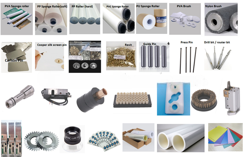
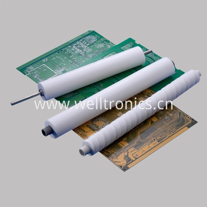
2. Process Cleaning
Before a board reaches the flying probes tester, it must be physically pristine. Micro-dust, fibers, and moisture residues are “silent killers” that lead to false failures or, worse, latent defects.
- PVA Sponge Rollers: In the wet process, these rollers ensure uniform de-watering. Any water spots left behind can lead to oxidation or chemical residues that interfere with PCB electrical test methods.
- Sticky Rollers: Before the imaging and testing phases, using a silicone or PE sticky roller removes micro-particles that could cause a probe to lose contact, triggering a false “open circuit” report.
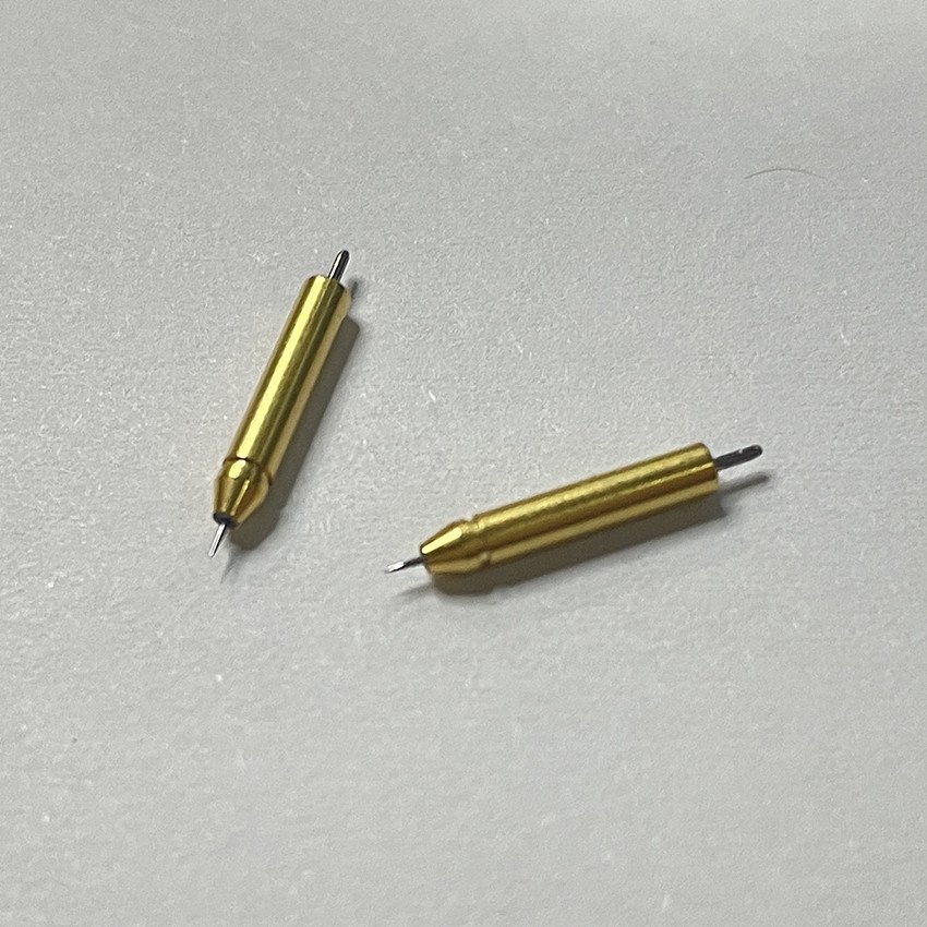
3. Precision Alignment: Unifying Coordinates with Locating Pins
A common cause of failure in a flying probe test for multilayer PCB is not a design flaw, but a mechanical alignment error. If the physical board is not perfectly synced with the digital CAD data, the probes will miss their targets.
The Role of Locating Pins
Locating Pins (including round and diamond locating pin types) are the anchors of the production line. They ensure that the coordinate system used during CNC drilling and routing is identical to the coordinate system used during electrical testing.
- Repeatability: High-quality pins prevent “play” or shifting of the board during high-speed movements.
- Accuracy: When the board is mechanically locked into place, the flying probe machine can execute its routine with micron-level precision, significantly increasing PCB fault detection efficiency.
4. The Final Gate: Flying Probe Testing
As boards become more complex and production runs become more customized, the industry has shifted significantly toward non-fixture circuit testing. This is where the flying tester becomes the hero of the production line.
What is Flying Probe Testing?
A flying probe machine uses highly mobile, high precision PCB test probes that move at high speeds across the X, Y, and Z axes. Unlike the traditional bed of nails test (which requires an expensive, custom-built fixture for every design), a flying probe is software-driven. You simply upload the Gerber or CAD data, and the machine “flies” its probes to the designated test points.
Advantages of the Flying Probe Machine
- No Fixture Costs: This is particularly beneficial for prototypes and small batches where the flying probe tester price is easily justified by the savings in custom hardware.
- Multilayer Precision: A flying probe test for multilayer PCB can detect internal shorts and opens that are invisible to the naked eye or AOI (Automated Optical Inspection).
- Sophisticated Diagnostics: Modern equipment, such as a Spea flying probe, performs not just continuity checks, but also LCR (Inductance, Capacitance, Resistance) measurements and even functional power-up tests.
Optimizing the Test
To maintain high throughput, automated PCB testing software optimizes the probe travel path. While the speed test of a flying probe is slower than a bed-of-nails for mass production, its ability to detect “latent” defects—defects that might only fail once the product is in the field—is far superior.
5. Integrating the Ecosystem: The Welleltron Edge
Building a zero-defect line is about the synergy between these four stages. When your Hitachi CMI data confirms the copper is perfect, your Sponge Rollers ensure the surface is clean, and your Locating Pins ensure the board is aligned, your flying probe testing results will move from “detecting defects” to “confirming perfection.”
Comparing PCB Electrical Test Methods
| Feature | Flying Probe Testing | Bed of Nails (Jig) |
| Setup Time | Minutes (Software upload) | Weeks (Fixture build) |
| Flexibility | Extremely High | Low |
| Pitch Support | Fine pitch (< 50 microns) | Limited by pin density |
| Best For | Flying probe test for multilayer PCB | High-volume, low-complexity |
6. Flying Probe vs. Bed of Nails
Choosing the right automated PCB testing equipment depends on your specific “GEO” (geographic market) and production volume.
| Feature | Flying Probe Test | Bed of Nails (Jig Testing) |
| Tooling Cost | $0 (Software based) | High (Custom fixture per design) |
| Setup Time | Minutes (CAD upload) | Days/Weeks (Fixture fabrication) |
| Testing Speed | Moderate | Very High |
| Pitch Capability | Ultra-fine (up to 50 microns) | Limited by probe density |
| Best For | Prototypes, HDI, High-mix | Mass production, Low-complexity |
For many modern factories, the flying probe test machine is the preferred choice for flying probe test for multilayer PCB because it offers the flexibility to adapt to rapid design changes without the lead time of traditional jigs.
Conclusion
The transition to a zero-defect PCB production line is a journey of precision. From the initial measurement of copper with Hitachi CMI instruments to the final validation using a flying probe tester, every step must be optimized for accuracy.