
Hitachi CMI165 Copper Thickness Tester
$3,300.00
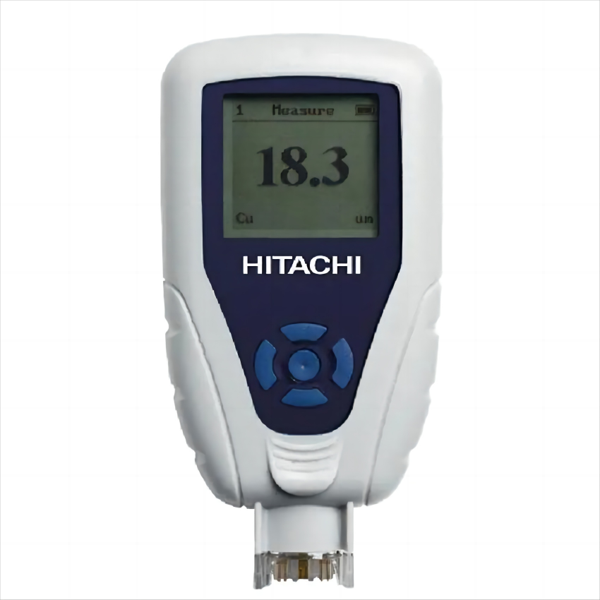
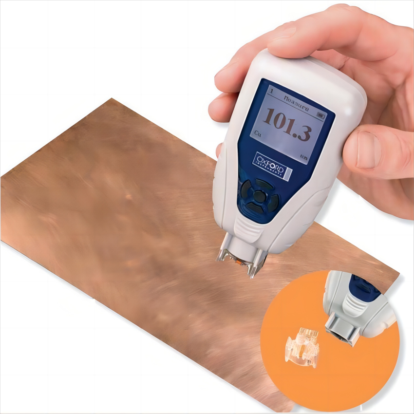
Hitachi CMI165 Copper Thickness Tester is a specialized, micro-resistance-based instrument designed for high-resolution, non-destructive measurement of ultra-thin copper thickness on PCB surfaces, often used for quality control in HDI manufacturing.
1. Overview of the Hitachi CMI165
The Hitachi CMI165 is a specialized digital thickness gauge that measures copper thickness on both rigid and flexible PCB materials. Unlike standard coating thickness gauges that might struggle with the conductivity of copper over various substrates, the CMI 165 is “substrate independent.” This means the thickness reading is not influenced by the laminate thickness or any copper layers on the opposite side of the board.
Designed with portability in mind, this thickness gauge meter allows for rapid testing directly on the production line. Whether you are auditing incoming copper-clad laminates (CCL) or checking the thickness of pcb board surfaces after the plating process, the CMI 165 provides the high precision thickness data required for high-reliability applications.
2. Core Functionality: Micro-Resistance Technology
The technical heart of the Hitachi CMI165 is its use of the Four-Point Probe micro-resistance method. This is the gold standard for measuring conductive layers on non-conductive substrates.
Key Features of the CMI165:
Automatic Temperature Compensation: Resistance is affected by temperature. The CMI 165 automatically adjusts its readings based on the ambient temperature, ensuring the thickness units remain consistent in both air-conditioned labs and hot plating shops.
Dual Mode Capability: The device can measure both Electroless Copper and Electrodeposited Copper, with user-selectable settings to account for the differing conductivity of these materials.
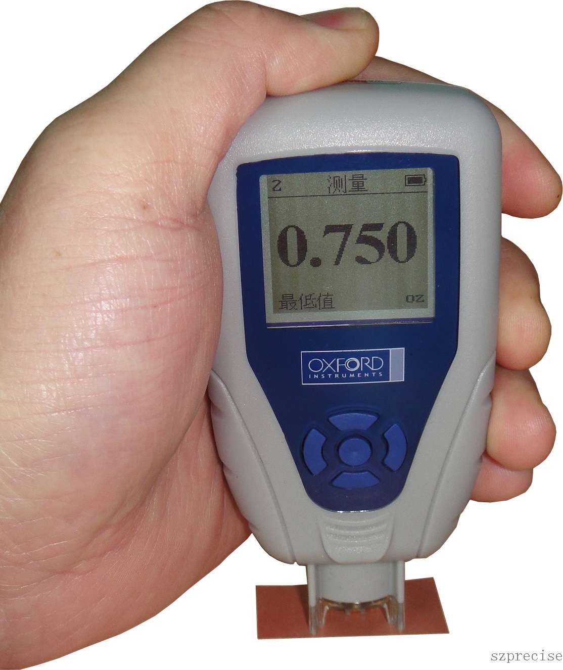
Digital Gauge Meter Display: The large, backlit gauge meter digital screen allows for easy reading in dark environments, displaying values in mils.
3. Industrial Applications in Electronics Manufacturing
The CMI165 is an essential thickness gauge tool across several stages of the PCB lifecycle.
Quality Control in PCB Fabrication
During the plating process, it is easy for copper to be distributed unevenly. Using the CMI 165 for pcb thickness measurement at multiple points on a panel allows engineers to identify “thin spots” before the board moves to the etching stage. This prevents the creation of weak traces that could lead to circuit failure.
Incoming Material Inspection
Manufacturers must verify that the standard pcb board thickness of the copper foil matches the supplier’s specifications. The CMI165 acts as a reliable thickness measurement instrument for auditing raw materials, ensuring that the standard pcb thickness (such as 0.5oz or 1oz copper) is accurate before production begins.
Surface Finishing Industry
For boards that require precious metal finishing, the base copper thickness must be correct. The CMI165 is a versatile thickness tool that ensures the foundation is solid before gold, silver, or tin is applied.
4. Technical Characteristics and Data Integrity
The CMI 165 is built for precision. Its data characteristics ensure that it remains a trusted thickness measurement tool for aerospace and medical electronics.
High Resolution: The digital thickness gauge provides readings down to 0.01 mils or 0.1 .
Repeatability: It offers exceptional consistency, with typical repeatability within 1% for standard electrodeposited copper.
Measurement Units: Users can easily toggle between different thickness measurement units (metric vs. imperial) to match customer requirements.
Calibration Memory: The device can store a Calibration Standard profile, making it easy to reset the device to factory or user-defined accuracy levels.
| CMI95M | CMI165 | CMI511(CMI500) | CMI563 | CMI760(CMI700) | |
| Technique | Microresistance | microresistance | Eddy curreny | microresistance | microresistance |
| Copper Foil | √ | √ | × | √ | √ |
| Copper Clad Laminate(CCL) | √ | √ | × | √ | √ |
| Copper-Surface | × | √ | × | √ | √ |
| Copper-Fineline | × | √ | × | √ | √ |
| Copper Thru-hole | × | × | √ | × | optional |
| Temperature Compensation | × | √ | √ | × | √ (ETP Probe) |
| Replacement Probe Tip | × | √ | × | √ | √ (SRP-4 Probe) |
| Unit Selection | oz or um | mil or um | mil or um | mil or um | mil or um |
| Thickness Range | 8 indicator lights 1/8-4 oz 5-140 um | Electroless Cu 0.01-0.5 mil 0.25-12.7 um Electroplated Cu 0.1-10 mil 2-254 um | 0.08-4.0 mil 2-102 um | Electroless Cu 0.01-0.5 mil 0.25-12.7 um Electroplated Cu 0.1-6 mil 3-152 um | Surface Cu 0.01-10 mil 0.25-254 um Thru-hole Cu 0.05-4 mil 1-102um |
FAQ
1. Which probe does the CMI165 use?
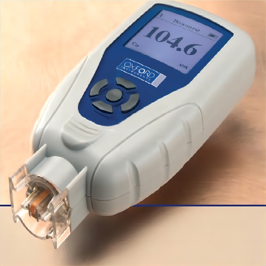
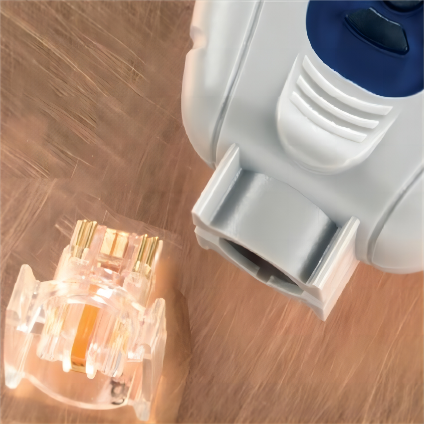
The brochure identifies the SRP-T1 probe, featuring a replaceable tip and illuminated measurement area. Confirm replacement-part compatibility using the instrument’s model and serial number.
2. How does the CMI165 measure copper thickness?
It uses a four-point electrical resistance method, also called microresistance. The probe contacts the copper surface, and the instrument converts the electrical measurement into a thickness reading. It is not an XRF analyzer.
3. What is the measurement range of the CMI165?
Hitachi’s brochure lists 0.25–12.7 µm for electroless copper and 2–254 µm for electroplated copper. Confirm the applicable range for your instrument configuration and sample before ordering.
4. Can the CMI165 measure copper inside plated through-holes?
The CMI165 is intended for surface and trace measurements. Do not assume its surface probe can measure hole-wall copper. For plated through-holes, specify a dedicated measurement system and provide the hole diameter, board thickness, and expected copper thickness.
5. Can the CMI165 measure fine copper traces?
Hitachi specifies etched traces as narrow as 204 µm. Suitability still depends on the sample geometry and correct probe placement.


 English
 German
 French
 Spanish
 Vietnamese
 Russian