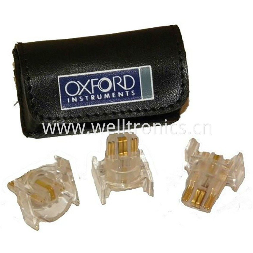

Hitachi Cmi165 Tips 51-SRP-T1
$230.00
Hitachi Cmi165 Tips is a high-purity micro-resistance contact designed specifically for the CMI165 tester, used for high-resolution non-destructive measurement of the thickness of ultra-thin copper layers on PCB surfaces.
Core Material: High-purity testing-grade crystal
Dimensions:Standard tip diameter
1.Hitachi Cmi165 Tips Overview
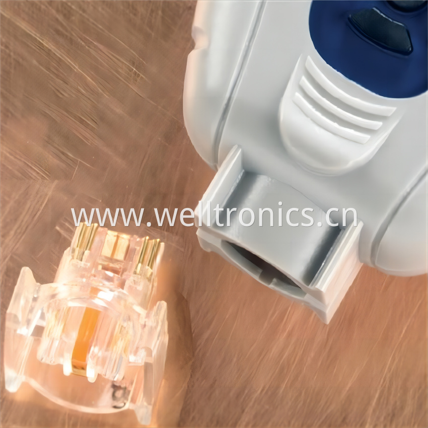
Hitachi Crystal Probe Tips for CMI165 Gauge (model 51-SRP-T1, also called Cmi165 Crystal Tips) are essential consumable components for Hitachi CMI165 Surface Cu Thickness Tester. As original Hitachi (Oxford) parts, these Crystal Tips are engineered to maintain the gauge’s high-precision measurement performance, critical for surface copper thickness testing in PCB manufacturing. The crystal material enables stable eddy current induction—key to accurate readings of electroless and electrodeposited copper layers. Compatible exclusively with the CMI165 probe head (CMI165 probe head), they integrate seamlessly with other testing accessories like Nylon Brush (for cleaning), calibration standard plate (for post-replacement calibration), and Antistatic PP Sheet (for storage), forming a reliable quality control chain for PCB copper testing.
2. Hitachi Cmi165 Tips MaterialandTechnology
The superior performance of the Hitachi Cmi165 Tips is rooted in advanced material science and application of the Micro-Resistance principle.
1. Material (High-Purity Alloy)
Composition: The tips are made from a proprietary high-purity conductive alloy. This material choice is critical to ensure a stable and repeatable electrical contact with the copper trace, minimizing the inherent electrical noise or “contact resistance.”
Wear Resistance: The material possesses excellent wear-resistant properties, crucial for maintaining tip geometry and accuracy over thousands of measurements, thus extending the CMI165 Tips lifetime before replacement is necessary.
2. Technical Principle (Targeted Micro-Resistance)
The Hitachi Cmi165 Tips utilizes a micro-resistance method, where the tips must:
Establish Stable Current Flow: The tips ensure that the small, controlled current flow necessary for the measurement is consistent across the copper trace.
Isolate Measurement: The tip’s geometry and contact area are meticulously designed to limit the measurement field, preventing interference from the substrate or adjacent fine traces—a critical factor for accurate HDI PCB Testing.
3. Key Features and Functional Characteristics
The design of the Hitachi Cmi165 Tips emphasizes precision, user-friendliness, and cost control.
| Feature | Description | Benefit |
| Micro-Contact Geometry | Extremely small, precise contact area. | Allows accurate measurement on narrow Copper Trace Thickness and micro-pads. |
| Seamless Compatibility | Guaranteed compatibility with the CMI165 instrument head. | Ensures proper calibration and eliminates the compatibility issues seen with Non-OEM CMI165 Tips. |
| Quick Replacement | Designed for fast, tool-free replacement by the operator. | Minimizes downtime, making the CMI165 Tips Replacement process efficient. |
| Low Maintenance | High material durability reduces the frequency of Tip Maintenance. | Lowers overall operational and consumable costs. |
4. Application Scenarios
The Hitachi Cmi165 Tips are indispensable in specific high-demand segments of the Electronics Manufacturing and Surface Finishing Industry:
HDI/High-Layer Count PCB Production: The primary application is measuring the thickness of the thin copper layers essential for micro-vias and fine-line circuitry, often in the <10μm range.
Chemical Copper Plating QC: Used to monitor and control the Electroless Copper deposition process, ensuring minimum thickness requirements are met before subsequent electroplating.
R&D Prototyping Labs: Essential for verifying copper thickness on newly designed boards and experimental plating processes, where accurate data is needed to correlate with electrical performance.


