
Identify What You Need to Measure
Surface Copper Thickness
Identify whether you need to measure copper foil, copper on laminate, or finished copper on pads and traces. Define the thickness range, tolerance, available measurement area, and production stage. A probe suitable for a broad exposed copper area may not work on a narrow trace or a coated surface, so provide the supplier with representative samples or drawings before selecting the instrument.
Plated Through-Hole Copper Thickness
PTH inspection measures copper deposited on the hole wall and requires a dedicated instrument with a compatible probe. Specify the finished hole diameter, board thickness, sample construction, and inspection locations. Confirm what region the probe evaluates and how the reading should be interpreted; a measurement should not automatically be treated as the minimum copper thickness everywhere inside the hole.
Overall PCB Thickness
Overall PCB thickness is the distance between the surfaces defined by the drawing. Clarify whether the requirement includes solder mask or other surface features, and identify suitable measurement locations. Choose a mechanical gauge or micrometer with appropriate contacts, measuring force, and reach, particularly for thin or flexible boards that may deform during measurement.
V-Score Remaining Thickness
V-score remaining thickness is the material left between opposing grooves, rather than the overall board thickness or either groove’s depth. Select a gauge whose contacts fit the groove and whose throat depth reaches the required inspection points. Confirm that the contacts reach the intended surfaces without resting on the groove flanks or bending the panel.
Surface-Finish Layer Thickness
Measuring nickel, gold, palladium, or another finish layer is a separate task from measuring PCB copper thickness. Define the complete coating stack, the individual layers requiring inspection, and the available measurement area. The selected system must distinguish the required layers under the actual sample conditions; a copper thickness gauge should not be assumed suitable for ENIG or ENEPIG layer measurement.
Start with the drawing and inspection requirement. Specify whether the measurement concerns an individual metal layer, the complete board, or material remaining after machining.
| Measurement requirement | What you need to establish | Instrument or method to evaluate |
|---|---|---|
| Copper foil or surface copper thickness | Thickness of copper at a defined surface location | Suitable microresistance or other validated copper measurement system |
| Plated through-hole copper thickness | Copper thickness in an accessible plated hole | Dedicated PTH copper thickness gauge with a compatible probe |
| Overall PCB thickness | Distance between specified opposing board surfaces | Suitable micrometer or mechanical PCB thickness tester |
| V-score remaining thickness | Material left between opposing score grooves | Dedicated V-score web gauge |
| Metallic surface-finish thickness | Thickness of specified layers in a coating stack | A coating-analysis method validated for that stack, such as an appropriate XRF system |
Match Technology to Measurement Requirements
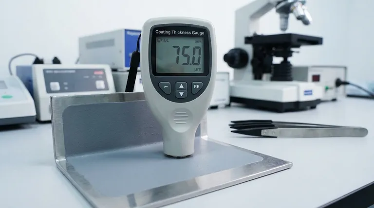
The term “digital thickness gauge” describes an interface, not a measurement capability. Two instruments can display micrometers while measuring different physical properties. Use the application and measurement principle to establish a shortlist.
| Measurement principle | PCB application to evaluate | Main checks before selection |
|---|---|---|
| Microresistance | Accessible surface copper, foil, pads, or traces | Conductor geometry, probe placement, surface condition, and supported thickness range |
| Application-specific eddy current | Plated through-hole copper | Compatible hole geometry, probe configuration, sample construction, and required settings |
| Mechanical contact | Overall board thickness | Reference surfaces, contact size, measuring force, and support |
| Specialized groove contacts | V-score remaining thickness | Groove access, contact alignment, throat depth, and panel clearance |
| Suitable coating analysis, such as XRF | Individual metallic finish layers | Layer stack, measurement area, calibration approach, and analysis limitations |
Microresistance for Surface Copper
Microresistance instruments use electrical measurements to determine copper thickness under defined conditions. Their suitability depends on the material, conductor geometry, and probe arrangement. Confirm the minimum measurement area, supported trace dimensions, temperature requirements, and permitted surface condition. A setup demonstrated on bare copper should not automatically be used after surface finishing.
Dedicated Systems for PTH Copper
PTH measurement requires an application-specific system rather than any gauge carrying an “eddy current” label. Hitachi’s official PCB comparison lists the CMI511 for through-hole copper and the CMI760 with optional through-hole capability, while the CMI165, CMI563, and CMI760 cover surface copper applications.
Mechanical Measurement for Board and V-Score Dimensions
Mechanical instruments measure separation between their contacts, so contact geometry determines which dimension is captured. Standard contacts may suit overall board thickness; V-score inspection needs contacts that enter the groove correctly.
Check Probe Fit and Measurement Access
A suitable measurement principle does not guarantee that the probe can reach the inspection point. Evaluate access on real boards, including the largest panel and the most restricted location.
- For surface copper: Check trace width, available contact area, nearby edges, coatings, and positioning requirements.
- For PTH copper: Verify the probe’s permitted hole dimensions and insertion procedure; never force a probe into a hole.
- For board thickness: Confirm that both contacts land on the specified surfaces without bridging unwanted features.
- For V-scores: Check contact profile, groove seating, upper-to-lower alignment, and usable throat depth.
- For populated boards: Consider interference from components, connectors, fixtures, and support structures.
Confirm compatibility using the instrument model and accessory part number. Similar connectors or appearance do not establish that a probe is suitable. During the trial, the operator should be able to position the sample without bending the PCB, loading the probe sideways, or making sensitive contacts support the panel’s weight.
Compare Performance Against the Inspection Tolerance
More display digits do not necessarily mean better measurement. Evaluate performance within the thickness range used in production, especially near acceptance limits.
| Specification | What it means | What to ask the supplier |
|---|---|---|
| Range | Supported thickness interval | Does the stated performance cover our working range? |
| Resolution | Smallest displayed increment | Is the increment suitable for our inspection requirement? |
| Error specification | Limits on the difference from reference values under stated conditions | Is the limit fixed, percentage-based, or a combination? |
| Repeatability | Variation under defined repeated-measurement conditions | Does the test include sample removal and repositioning? |
| Measurement uncertainty | Quantified uncertainty associated with the result | Does the evaluation represent our sample and method? |
Avoid adopting an arbitrary resolution-to-tolerance ratio as the only selection rule. Consider the complete measurement method, including operator handling and sample variation. Establish a decision rule for results close to a limit, and do not repeatedly measure a part until one reading happens to pass.
Match the Thickness Gauge to the Manufacturing Stage
Incoming Inspection
Determine whether the task is material classification or numerical thickness verification. Sorting foil into categories is different from recording a measured value against a tolerance. Select a system that provides the required result and allows it to be linked to the incoming material lot.
In-Process Inspection
Define the sample condition, measurement locations, and handling procedure at the chosen production stage. Follow the instrument’s requirements for cleanliness, temperature, and preparation. Consistent locations help distinguish process changes from normal differences across a panel; temperature compensation, where provided, does not remove the need to follow the operating limits.
Final QC Inspection
Finished boards may have coatings, restricted access, or components that prevent the original measurement method from being used. Confirm that the method remains valid. If an approved coupon is used instead, document how it represents the product and how its results support acceptance.
Frequently Asked Questions PCB Thickness Gauge
Can One Gauge Measure Every PCB Thickness?
Generally, different features require different methods or configurations. Some systems support surface and through-hole copper with appropriate probes, but overall board thickness and V-score remaining thickness involve separate mechanical measurements.
Can a Standard Caliper copper thickness measurement on a Finished PCB?
A standard caliper generally measures the combined dimension between its jaws. It does not isolate an individual copper layer on a finished PCB. Use a method designed and validated for the required layer measurement.
Is a Handheld Gauge Less Accurate Than a Benchtop Instrument?
The format alone does not establish accuracy. Compare specified performance and results from representative samples. A supported bench setup may improve positioning for some tasks, while a handheld instrument may better suit inspection across several stations.
What information should I send a gauge supplier?
Provide the measurement target, thickness range, tolerance, stackup, feature dimensions, production stage, inspection locations, and expected workload. Representative boards or coupons allow the supplier to demonstrate whether the proposed system meets those requireme
 Russian
 English
 German
 French
 Spanish
 Vietnamese