PCB Artwork Protective Film
$130.00 / Set
PCB protective film is purpose fully pressed a protective layer on the diazo film or silver halide film to prevent the film from chafing and extend the lifespan of artwork film.
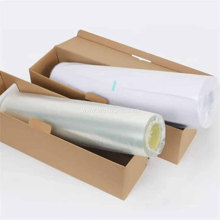
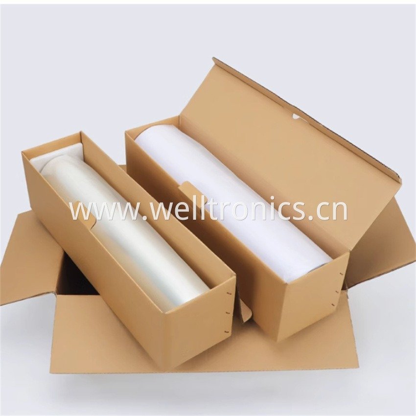
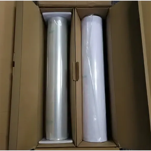
Size:20″*150mtr, 22″*150mtr,24″*150mtr and other size customized
1.PCB Artwork Protective Film Overview
The PCB Artwork Protective Film acts as a Surface Guard for the diazo film(silver halid film). It is typically a Self-Adhesive Film applied to large PCB panels immediately after processes like etching or final surface treatment, ensuring the delicate copper features remain pristine before soldering or final assembly.
Definition: A polymer-based protection film designed with a specific Adhesive Strength to temporarily shield the PCB surface, providing PCB protection against physical abrasion, dust, and corrosive elements, with the ability for Residue-Free Peel-off.
Search Intent: Users often search for “pcb film” or “protection film price” when looking for cost-effective ways to minimize in-process damage and rework.
2. Material Technology and Key Characteristics
The composition of PCB Artwork Protective Film must balance adhesion, protection, and clean removal, especially within the demanding manufacturing environment.
1. Material (PE Protective Film & PET Protective Film)
Polyethylene PCB Film (PE): Commonly used for general PCB Shipping Film and temporary handling protection due to its flexibility and low cost. It often features a Clear Protective Film or Blue Protective Film color.
PET Protective Film: Preferred for applications requiring higher tensile strength, temperature resistance, or chemical stability, making it suitable for more critical PCB Process Film stages.
PI Protective Film: While not typical for large area artwork protection, PI Protective Film (Polyimide) is used for highly localized, high-heat applications like Gold Finger Protection Film during reflow or specialized Solder Masking Film.
2. Adhesive Technology
The use of a precise Low-Tack Adhesive (often acrylic- or silicone-based) is crucial. Unlike strong industrial adhesives, this film must guarantee a Residue-Free Peel after removal, as any residue can interfere with subsequent plating or soldering processes.
3. Specialty Features
Anti-Static Protective Film / ESD Protective Film: Essential for protecting static-sensitive electronic components and traces from electrostatic discharge during handling.
Anti-Corrosion Film: Contains volatile corrosion inhibitors (VCIs) to shield exposed copper surfaces from oxidation during long-term storage or shipment in humid environments.
3. Key Features and Advantages
The specialized features of these films translate directly into cost savings and quality assurance.
| Feature | Advantage in PCB Manufacturing | Value for Purchasers |
| Residue-Free Peel | Prevents contamination of gold plating pads or solderable areas. | Eliminates costly cleaning steps and prevents soldering defects. |
| Controlled Adhesive Strength | Allows the film to adhere during complex processes but detach easily. | Reduces labor time for removal and minimizes the risk of lifting delicate traces. |
| Wide Process Tolerance | Selection of High Temperature Protective Film options (e.g., Silicone Adhesive Film) available for heat-intensive stages. | Enables use in light PCB Rework Masking scenarios without melting or leaving carbonized residue. |
| Visual Inspection | Transparent PCB Film allows operators to visually inspect the underlying traces and surface quality without removing the film. | Speeds up in-process inspection and reduces manual handling. |
4. Application Scenarios
The film is deployed across various stages where the PCB is vulnerable to physical or chemical damage:
Transport and Storage: Applied as a Polyethylene PCB Film (PE) after final surface finish (e.g., ENIG or HASL) to prevent scratches, dust, and environmental tarnish before assembly.
Assembly Preparation: Used before component placement to protect solderable areas while surrounding surfaces are handled or cleaned.
Gold Finger Protection: Specific, thicker Gold Finger Protection Film is used during immersion gold or nickel plating to mask areas not intended for the process.
Rework and Repair: Applied as a Temporary Masking Film around a defective area during spot cleaning or thermal rework to prevent damage to nearby components or traces.
| Material | PET |
| Size | 20″*150mtr,22″*150mtr,24″*150mtr and other size customized |
| Usage | protect the artwork diazo film and silver halide film, it can used on both solder mask and circuits process |
| MOQ | 1 set |

")

")


